DEC J-11 processors
Introduction: 1983
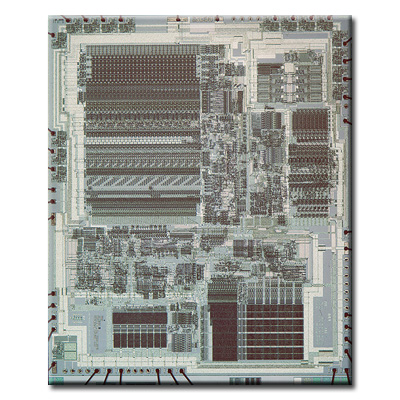
The J-11 (code name Jaws, which the design team never used) was DEC's fourth and last PDP-11 microprocessor design, and the first to be done in CMOS. The project was co-developed with Harris Semiconductor. Bob Supnik was the project leader through 1981, then Dan Casaletto. Paul Rubinfeld was lead engineer on the Data chip, Gil Wolrich on the Control chip and the FPA. Keith Henry wrote the microcode. Circuit design and layout were done by Harris Semiconductor.
The J-11 was intended to put a "capstone" on the PDP-11 family by providing the full functionality and performance of the PDP-11/70 in a microprocessor. Accordingly, the J-11 incorporated most of the architectural ornamentation from the 11/70 - dual register sets, data space, supervisor mode - as well as more modern inventions such as SMP support. Microcode-based floating point was standard, with accelerated floating point available as an option. CIS microcode was also intended to be an option.
The J-11 was a chip set consisting of three designs, one of which could be replicated: the Control chip (up to three supported), the Data chip, and the optional FPA chip. The Control and Data chips were implemented in Harris double-poly 4µ P-well CMOS. The FPA was implemented in DEC's double-metal 3µ NMOS process (ZMOS).
The J-11 was introduced late in 1983 at 3.75Mhz; subsequent tweaks pushed the performance to 4.5Mhz. The FPA was introduced in 1984. The FPA was used as the basis for the MicroVAX Floating Point Unit and the V-11 F chip.
Source: Unknown.


