
Intel 80486 processors
Introduction: April 1989 (80486DX), April 1991 (80486SX), March 1992 (80486DX2), November 1992 (80486SL), March 1994 (80486DX4)
In the race for more speed, the Intel 80486 (normally abbreviated as 486) was another major leap forward. The additional power available in the 486 fueled tremendous growth in the software industry. Tens of millions of copies of Windows, and millions of copies of OS/2, have been sold largely because the 486 finally made the GUI of Windows and OS/2 a realistic option for people who work on their computers every day.
The 486 chip is about twice as fast as the 386, which means that a 386DX-40 is about as fast as a 486SX-20. This made the 486 a much more desirable option, primarily because it could more easily be upgraded to a DX2 or DX4 processor at a later time. You can see why the arrival of the 486 rapidly killed off the 386 in the marketplace.
The 486 is now offered by Intel only for use in embedded microprocessor applications, used primarily in expansion cards.
Most of the 486 chips were offered in a variety of maximum speed ratings, varying from 16MHz up to 120MHz. Additionally, 486 processors have slight differences in overall pin configurations. The DX, DX2, and SX processors have a virtually identical 168-pin configuration, whereas the OverDrive chips have either the standard 168-pin configuration or a specially modified 169-pin OverDrive (sometimes also called 487SX) configuration. If your motherboard has two sockets, the primary one likely supports the standard 168-pin configuration, and the secondary (OverDrive) socket supports the 169-pin OverDrive configuration. Most newer motherboards with a single ZIF socket support any of the 486 processors except the DX4. The DX4 is different because it requires 3.3v to operate instead of 5v, like most other chips up to that time. A processor rated for a given speed always functions at any of the lower speeds. A 100MHz-rated 486DX4 chip, for example, runs at 75MHz if it is plugged into a 25MHz motherboard. Note that the DX2/OverDrive processors operate internally at two times the motherboard clock rate, whereas the DX4 processors operate at two, two-and-one-half, or three times the motherboard clock rate.
The 486-processor family is designed for greater performance than previous processors because it integrates formerly external devices, such as cache controllers, cache memory, and math coprocessors. Also, 486 systems were the first designed for true processor upgradability. Most 486 systems can be upgraded by simple processor additions or swaps that can effectively double the speed of the system.
486DX processors


The original Intel 486DX processor was introduced on April 10, 1989, and systems using this chip first appeared during 1990. The first chips had a maximum speed rating of 25MHz; later versions of the 486DX were available in 33MHz- and 50MHz-rated versions. The 486DX originally was available only in a 5v, 168-pin PGA version, but now is also available in 5v, 196-pin PQFP (Plastic Quad Flat Pack), and 3.3v, 208-pin SQFP (Small Quad Flat Pack). These latter form factors are available in SL Enhanced versions, which are intended primarily for portable or laptop applications in which saving power is important.
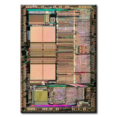
The 486DX processor is fabricated with low-power CMOS (complementary metal oxide semiconductor) technology. The chip has a 32-bit internal register size, a 32-bit external data bus, and a 32-bit address bus. These dimensions are equal to those of the 386DX processor. The internal register size is where the "32-bit" designation used in advertisements comes from. The 486DX chip contains 1.2 million transistors on a piece of silicon no larger than your thumbnail. This figure is more than four times the number of components on 386 processors and should give you a good indication of the 486 chips relative power.
The standard 486DX contains a processing unit, a floating-point unit (math coprocessor), a memorymanagement unit, and a cache controller with 8KB of internal-cache RAM. Due to the internal cache and a more efficient internal processing unit, the 486 family of processors can execute individual instructions in an average of only two processor cycles. Compare this figure with the 286 and 386 families, both of which execute an average 4.5 cycles per instruction. Compare it also with the original 8086 and 8088 processors, which execute an average 12 cycles per instruction.
At a given clock rate (MHz), therefore, a 486 processor is roughly twice as efficient as a 386 processor; a 16MHz 486SX is roughly equal to a 33MHz 386DX system; and a 20MHz 486SX is equal to a 40MHz 386DX system. Any of the faster 486s are way beyond the 386 in performance. The 486 is fully instruction-set-compatible with previous Intel processors, such as the 386, but offers several additional instructions (most of which have to do with controlling the internal cache). Like the 386DX, the 486 can address 4GB of physical memory and manage as much as 64TB of virtual memory.
Under an operating system such as Windows or OS/2, therefore, both 16-bit and 32-bit programs can run simultaneously on this processor with hardware memory protection. If one program crashes, the rest of the system is protected, and you can reboot the blown portion through various means, depending on the operating software.
The 486DX series has a built-in math coprocessor that sometimes is called an MCP (math coprocessor) or FPU (floating-point unit). This series is unlike previous Intel CPU chips, which required you to add a math coprocessor if you needed faster calculations for complex mathematics. The FPU in the 486DX series is 100 percent software-compatible with the external 387 math coprocessor used with the 386, but it delivers more than twice the performance. It runs in synchronization with the main processor and executes most instructions in half as many cycles as the 386.
486SX processors

The 486SX, introduced in April 1991, was designed to be sold as a lower-cost version of the 486. The 486SX is virtually identical to the full DX processor, but the chip does not incorporate the FPU or math coprocessor portion. As you read earlier in this chapter, the 386SX was a scaled-down (some people would say crippled) 16-bit version of the full-blown 32-bit 386DX. The 386SX even had a completely different pinout and was not interchangeable with the more powerful DX version. The 486SX, however, is a different story. The 486SX is, in fact, a full-blown 32-bit 486 processor that is basically pin-compatible with the DX. A few pin functions are different or rearranged, but each pin fits into the same socket.
The 486SX chip is more a marketing quirk than new technology. Early versions of the 486SX chip actually were DX chips that showed defects in the math-coprocessor section. Instead of being scrapped, the chips were packaged with the FPU section disabled and sold as SX chips. This arrangement lasted for only a short time; thereafter, SX chips got their own mask, which is different from the DX mask (a mask is the photographic blueprint of the processor and is used to etch the intricate signal pathways into a silicon chip). The transistor count dropped to 1.185 million (from 1.2 million) to reflect this new mask.
The 486SX chip is twice as fast as a 386DX with the same clock speed. Intel marketed the 486SX as being the ideal chip for new computer buyers, because fewer entry-level programs of that day used math-coprocessor functions.
The 486SX was normally available in 16, 20, 25, and 33MHz-rated speeds, and there was also a 486 SX/2 that ran at up to 50 or 66MHz. The 486SX normally comes in a 168-pin version, although other surface-mount versions are available in SL-enhanced models. Despite what Intels marketing and sales information implies, no technical provision exists for adding a separate math coprocessor to a 486SX system; neither is a separate math coprocessor chip available to plug in. Instead, Intel wanted you to add a new 486 processor with a built-in math unit and disable the SX CPU that already was on the motherboard.
486SL processors
The 486SL was a short-lived, standalone chip. The SL enhancements and features became available in virtually all the 486 processors (SX, DX, and DX2) in what are called SL enhanced versions. SL enhancement refers to a special design that incorporates special power-saving features. The SL enhanced chips originally were designed to be installed in laptop or notebook systems that run on batteries, but they found their way into desktop systems, as well. The SL-enhanced chips featured special power-management techniques, such as sleep mode and clock throttling, to reduce power consumption when necessary. These chips were available in 3.3v versions, as well.
Intel designed a power-management architecture called system management mode (SMM). This mode of operation is totally isolated and independent from other CPU hardware and software. SMM provides hardware resources such as timers, registers, and other I/O logic that can control and power down mobile-computer components without interfering with any of the other system resources. SMM executes in a dedicated memory space called system management memory, which is not visible and does not interfere with operating system and application software. SMM has an interrupt called system management interrupt (SMI), which services power-management events and is independent from, and higher priority than, any of the other interrupts. SMM provides power management with flexibility and security that were not available previously. For example, an SMI occurs when an application program tries to access a peripheral device that is powered down for battery savings, which powers up the peripheral device and reexecutes the I/O instruction automatically.
Intel also designed a feature called Suspend/Resume in the SL processor. The system manufacturer can use this feature to provide the portable computer user with instant-on-and-off capability. An SL system typically can resume (instant on) in one second from the suspend state (instant off) to exactly where it left off. You do not need to reboot, load the operating system, load the application program, and then load the application data. Simply push the Suspend/Resume button and the system is ready to go.
The SL CPU was designed to consume almost no power in the suspend state. This feature means that the system can stay in the suspend state possibly for weeks and yet start up instantly right where it left off. An SL system can keep working data in normal RAM memory safe for a long time while it is in the suspend state, but saving to a disk still is prudent.
486 OverDrive processors

On March 3, 1992, Intel introduced the DX2 speed-doubling processors. On May 26, 1992, Intel announced that the DX2 processors also would be available in a retail version called OverDrive. Originally, the OverDrive versions of the DX2 were available only in 169-pin versions, which meant that they could be used only with 486SX systems that had sockets configured to support the rearranged pin configuration. On September 14, 1992, Intel introduced 168-pin OverDrive versions for upgrading 486DX systems. These processors could be added to existing 486 (SX or DX) systems as an upgrade, even if those systems did not support the 169-pin configuration. When you use this processor as an upgrade, you install the new chip in your system, which subsequently runs twice as fast.
The DX2/OverDrive processors run internally at twice the clock rate of the host system. If the motherboard clock is 25MHz, for example, the DX2/OverDrive chip runs internally at 50MHz; likewise, if the motherboard is a 33MHz design, the DX2/OverDrive runs at 66MHz. The DX2/OverDrive speed doubling has no effect on the rest of the system; all components on the motherboard run the same as they do with a standard 486 processor. Therefore, you do not have to change other components (such as memory) to accommodate the double-speed chip. The DX2/OverDrive chips have been available in several speeds.
The Pentium OverDrive Processor became available in 1995. An OverDrive chip for 486DX4 systems had been planned, but poor marketplace performance of the SX2/DX2 chip meant that it never saw the light of day. One thing to keep in mind about the 486 Pentium OverDrive chip is that although it is intended primarily for SX2 and DX2 systems, it should work in any upgradable 486SX or DX system that has a Socket 2 or Socket 3.
Source: Upgrading and Repairing PCs (13th Edition) by Scott Mueller.