
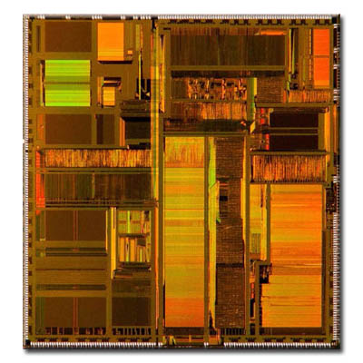
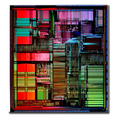
Intel Pentium (P5, P54, P54C, P54CS, P55C) processors
Introduction: March 1993 (P5), October 1993 (P54), March 1995 (P54C and P55C), June 1995 (P54CS), August 1997 (Tillamook)
Overview
On October 19, 1992, Intel announced that the fifth generation of its compatible microprocessor line (code-named P5) would be named the Pentium processor rather than the 586, as everybody had been assuming. Calling the new chip the 586 would have been natural, but Intel discovered that it could not trademark a number designation, and the company wanted to prevent other manufacturers from using the same name for any clone chips that they might develop. The first Pentium chip was shipped on March 22, 1993. Systems that use these chips were only a few months behind.
The Pentium was fully compatible with previous Intel processors, but it also differed from them in many ways. At least one of these differences was revolutionary: the Pentium featured twin data pipelines, which enabled it to execute two instructions at the same time. The 486 and all preceding chips performed only a single instruction at a time. Intel called the capability to execute two instructions at the same time superscalar technology. This technology provided additional performance compared with the 486. The standard 486 chip was able to execute a single instruction in an average of two clock cycles - cut to an average of one clock cycle with the advent of internal clock multiplication used in the DX2 and DX4 processors. With superscalar technology, the Pentium was able to execute many instructions at a rate of two instructions per cycle. Superscalar architecture usually was associated with high-output RISC (Reduced Instruction Set Computer) chips. The Pentium was one of the first CISC (Complex Instruction Set Computer) chips to be considered superscalar. The Pentium was almost like having two 486 chips under the hood.
The Pentium had a 32-bit address bus width, giving it the same 4GB memory-addressing capabilities as the 386DX and 486 processors. But the Pentium expanded the data bus to 64 bits, which meant that it was able to move twice as much data into or out of the CPU, compared with a 486 of the same clock speed. The 64-bit data bus required that system memory be accessed 64 bits wide, which meant that each bank of memory is 64 bits.
Even though the Pentium had a 64-bit data bus that transfered information 64 bits at a time into and out of the processor, the Pentium had only 32-bit internal registers. As instructions were being processed internally, they were broken down into 32-bit instructions and data elements, and processed in much the same way as in the 486. Some people thought that Intel was misleading them by calling the Pentium a 64-bit processor, but 64-bit transfers did indeed take place. Internally, however, the Pentium had 32-bit registers that were fully compatible with the 486.
The Pentium had two separate internal 8KB caches, compared with a single 8KB or 16KB cache in the 486. The cache-controller circuitry and the cache memory were embedded in the CPU chip. The cache mirrored the information in normal RAM by keeping a copy of the data and code from different memory locations. The Pentium cache was also able to hold information to be written to memory when the load on the CPU and other system components was less.
Systems based on the Pentium benefited greatly from secondary processor caches (L2), which usually consisted of up to 512KB or more of extremely fast (15 ns or less) Static RAM (SRAM) chips. When the CPU fetches data that was not already available in its internal processor (L1) cache, wait states slowed the CPU. If the data already was in the secondary processor cache, however, the CPU was able to go ahead with its work without pausing for wait states.
The Pentium used a BiCMOS (bipolar complementary metal oxide semiconductor) process and superscalar architecture to achieve the high level of performance expected from the chip. BiCMOS added about 10 percent to the complexity of the chip design, but added about 3035 percent better performance without a size or power penalty.
All Pentium processors were SL enhanced, meaning that they incorporated the SMM to provide full control of power-management features, which helped reduce power consumption. The second-generation Pentium processors (75MHz and faster) incorporated a more advanced form of SMM that included processor clock control. This allowed to throttle the processor up or down to control power use. It was also able to stop the clock, putting the processor in a state of suspension that required very little power. The second-generation Pentium processors ran on 3.3V power (instead of 5V), reducing power requirements and heat generation even further.
The Pentium, like the 486, contained an internal math coprocessor or FPU. The FPU in the Pentium had been rewritten and performed significantly better than the FPU in the 486, yet it was fully compatible with the 486 and 387 math coprocessor. The Pentium FPU was estimated at two to as much as 10 times faster than the FPU in the 486. In addition, the two standard instruction pipelines in the Pentium provided two units to handle standard integer math (the math coprocessor handled only more complex calculations). Other processors, such as the 486, had only a single-standard execution pipe and one integer math unit. Interestingly, the Pentium FPU contained a flaw that received widespread publicity...
Probably the most famous processor bug in history was the now legendary flaw in the Pentium FPU. It had often been called the FDIV bug, because it affects primarily the FDIV (floating-point divide) instruction, although several other instructions that use division are also affected. Intel officially refered to this problem as Errata No. 23, titled "Slight precision loss for floating-point divides on specific operand pairs." The bug had been fixed in the D1 or later steppings of the 60/66MHz Pentium processors, as well as the B5 and later steppings of the 75/90/100MHz processors. The 120MHz and higher processors were manufactured from later steppings, which did not include this problem.
The first-generation Pentium (P5) family

The Pentium had been offered in three basic designs, each with several versions. The first-generation design, came in 60 and 66MHz processor speeds. This design used a 273-pin PGA form factor and ran on 5v power. In this design, the processor ran at the same speed as the motherboard - in other words, a 1x clock was used.
The first-generation Pentium was created through an 0.8 micron BiCMOS process. Unfortunately, this process, combined with the 3.1 million transistor count, resulted in a die that was overly large and complicated to manufacture. As a result, reduced yields kept the chip in short supply; Intel was not able to make them fast enough. The 0.8 micron process was criticized by other manufacturers, including Motorola and IBM, which had been using 0.6 micron technology for their most advanced chips. The huge die and 5V operating voltage caused the 66MHz versions to consume up to an incredible 3.2 amps or 16 watts of power, resulting in a tremendous amount of heat and problems in some systems that did not employ conservative design techniques. Fortunately, adding a fan to the processor solved most cooling problems, as long as the fan kept running.
Much of the criticism leveled at Intel for the first-generation Pentium was justified. Some people realized that the first-generation design was just that; they knew that new Pentium versions, made in a more advanced manufacturing process, were coming. Many of those people advised against purchasing any Pentium system until the second-generation version became available.
The second-generation Pentium (P54, P54C, P54CS) family

Intel announced the second-generation Pentium on March 7, 1994. This new processor was introduced in 90 and 100MHz versions, with a 75MHz version not far behind. Eventually, 120, 133, 150, 166, and 200MHz versions were also introduced. The second-generation Pentium used 0.6 micron (75/90/100MHz) BiCMOS technology to shrink the die and reduce power consumption. The newer, faster 120MHz (and higher) second-generation versions incorporated an even smaller die built on a 0.35 micron BiCMOS process. These smaller dies were not changed from the 0.6 micron versions; they were basically a photographic reduction of the P54C die. Additionally, these new processors ran on 3.3V power. The 100MHz version consumed a maximum 3.25 amps of 3.3V power, which equals only 10.725 watts. Further up the scale, the 150MHz chip used 3.5 amps of 3.3V power (11.6 watts); the 166MHz unit drew 4.4 amps (14.5 watts); and the 200MHz processor used 4.7 amps (15.5 watts).
The second-generation Pentium processors came in a 296-pin SPGA form factor that was physically incompatible with the first-generation versions. The only way to upgrade from the first generation to the second was to replace the motherboard. The second-generation Pentium processors also had 3.3 million transistors - more than the earlier chips. The extra transistors existed because additional clockcontrol SL enhancements were added, along with an on-chip Advanced Programmable Interrupt Controller (APIC) and dual-processor interface.
The APIC and dual-processor interface were responsible for orchestrating dual-processor configurations in which two second-generation Pentium chips were able to process on the same motherboard simultaneously. Many of the Pentium motherboards designed for file servers came with dual Socket 7 specification sockets, which fully supported the multiprocessing capability of the new chips. Software support for what usually was called Symmetric Multi-Processing (SMP) was being integrated into operating systems such as Windows NT and OS/2.
The second-generation Pentium processors used clock-multiplier circuitry to run the processor at speeds faster than the bus. The 150MHz Pentium processor, for example, was able to run at 2.5 times the bus frequency, which normally was 60MHz. The 200MHz Pentium processor was able to run at a 3x clock in a system using a 66MHz bus speed.
A single-chip OverDrive upgrade was offered for second-generation Pentiums. These OverDrive chips were fixed at a 3x multiplier; they replaced the existing Socket 5 or 7 CPU, increased processor speed up to 200MHz (with a 66MHz motherboard speed), and added MMX capability, as well. Simply stated, this meant that a Pentium 100, 133, or 166 system equipped with the OverDrive chip had a processor speed of 200MHz. Perhaps the best feature of these Pentium OverDrive chips was that they incorporated MMX technology. MMX provided greatly enhanced performance while running the multimedia applications that were so popular today.
The Pentium MMX (P55C) family

The P55C (or 80503) was developed by Intel's Research & Development Center in Haifa, Israel. It was sold as Pentium with MMX Technology (usually just called Pentium MMX); although it was based on the P5 core (the 0.35 µm process was also used for this series) it featured a new set of 57 "MMX" instructions intended to improve performance on multimedia tasks, such as encoding and decoding digital media data.
The new instructions worked on new data types: 64-bit packed vectors of either eight 8-bit integers, four 16-bit integers, two 32-bit integers, or one 64-bit integer. So, for example, the PADDUSB (Packed ADD Unsigned Saturated Byte) instruction added two vectors, each containing eight 8-bit unsigned integers together, pairwise; each addition that would overflow saturated, yielding 255, the maximum unsigned value that was represented in a byte. These rather specialized instructions generally required special coding by the programmer for them to be used. MMX did not achieve significant popularity until after the P55C's lifetime.
The performance of the P55C improved over previous versions by a doubling of the Level 1 CPU cache from 16KB to 32KB.
The Pentium MMX (Tillamook) family
Pentium P55C notebook CPUs used a "mobile module" that held the CPU. This module was a PCB with the CPU directly attached to it in a special smaller form factor. The module snapped to the notebook motherboard and typically a heat spreader plate was installed and made contact with the module. Such notebooks frequently used the Intel 430MX chipset, a feature-reduced 430FX. However, with the 0.25 µm Tillamook Mobile Pentium MMX (named after a city in Oregon), the module also held the 430TX chipset along with the system's 512KB SRAM cache memory.
Source: Upgrading and Repairing PCs (13th Edition) by Scott Mueller.
Source: Wikipedia, the free encyclopedia.