
Samsung Alpha 21364 (EV7) processors
Introduction: January 2002
The first news about the architecture of 21364 (EV7) was from a Microprocessor Forum in October of 1998. It said that the processor would be based upon the core of EV6 but with a Direct Rambus DRAM controller (presumably, 4-channel) and a L2 cache (1.5MB write-back 6-way set associative) both integrated. It was also mentioned that no core modifications were planned, though could be another reason: no one could handle this hard task because not so many processor designing engineers were employed by Compaq those days. The design was expected to be completed by 2000.
Hewlett-Packard inherited the Alpha architecture after the acquisition of Compaq, though didn't need that bequest in fact. It developed the PA-RISC (Precision Architecture RISC) architecture on its own and held an alliance with Intel to develop the IA-64 architecture (renamed to the Itanium architecture later). So, HP's actions regarding the Alpha architecture were limited to selling EV6/EV67/EV68-based servers inherited from Compaq and launching EV7 into production. Anyway, EV7 was presented finally in January of 2002.
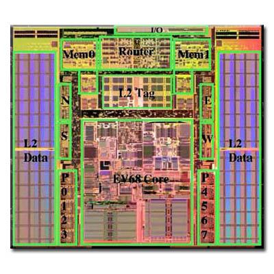
As it had been expected, EV7 contained the core of EV68 with no modifications at all, also several units integrated additionally: two operating memory controllers (two Z-boxes, for Direct Rambus DRAM PC800), a multifunctional router (R-box, for multiprocessor support and networking) and a full-speed L2 cache memory (S-cache, 1.75MB write-back 7-way set associative). The data path to S-cache was 128-bit wide and the cache itself operated with significant latencies (12 cycles while reading). Both Z-boxes and R-box were clocked at 2/3 of a core frequency. Operating memory channels' speed depended on Z-boxes and was 1/2 of their frequency (1/3 of a core frequency respectively), though was DDR capable.
Every Z-box supported 5 memory channels (4 primary and 1 auxiliary) 18-bit wide each (16 bits for commands/data/addresses and 2 bits for ECC). The auxiliary channel was optional and could be used to organise a failure-tolerant memory array (roughly speaking, like RAID3). For example, a quad-word (64 bits) written to memory was divided for 4 words and each of them was sent through a dedicated channel, and the auxiliary one was used to store a checksum. In addition, every Z-box could hold up to 1024 memory pages open. The total theoretical operating memory bandwidth of one EV7 was 12.8GB/s given DR DRAM PC800 at the standard frequency, an impressive figure if compared to 2.66GB/s of 256-bit 83MHz SDRAM found usually in dual-processor systems of the previous generation. Every EV7 in a multiprocessor system controlled an operating memory area of its own, so such a memory model was NUMA (Non-Uniform Memory Access), not a traditional SMP (Symmetrical MultiProcessing) also known as UMA (Uniform Memory Access). The latter implied all processors installed in a particular system to have access to a single (common) operating memory area. So, every EV7 processor (128 maximum) in a system could access memory through controllers of its own as well as through other processors' controllers.
R-box carried a communicative function between processors, also between a particular processor and local peripherals. There were 4 independent channels with a theoretical bandwidth of 6GB/s each (one per every neighbourous processor connected), also 1 additional channel for high-speed input/output transfers. There was a companion chip called IO7 to serve as a bridge between a processor and peripherals. It included support for three PCI or PCI-X buses and one AGP bus. A particular system could include as many IO7 chips as there were EV7 processors present.
21364 processors could be connected to each other using various algorithms, but so-called torus and shuffle interconnects were chosen usually. Besides, the second one was more effective in some situations. For example, considering 8-processor systems, shuffle allowed each processor to be connected straightforward to 4 others while torus - to 3 others only. A good guess that for 16-processor and more powerful systems this difference vanished.
21364 (EV7) was manufactured using a 7-layer 0.18µ CMOS process. Consisted of 152M transistors (including 137M spent on I-cache, D-cache and S-cache), therefore utilised a very large die size of 397mm². Prototypes were clocked at 1250MHz (TDP of 155W), though those processors installed in production systems by HP were running at lower speeds (1000MHz in AlphaServer DS25, ES47 and ES80, 1150MHz in AlphaServer GS1280 and SC1280). In fact, EV7 was a quick hack of EV6 to allow for better scalability, and not an engineering wonder definitely. However, it took whole 4 years for first samples to appear, so either Compaq was a poor developer or it didn't care about EV7 almost at all.
In December of 2002, Hewlett-Packard let go out a press-release saying that first EV7-based servers would be available in January of 2003. Later, 21364A (EV79) ought to be produced using a 0.13µ SOI process, and there were no further Alpha processors planned. In March of 2003, a prototype of EV79 was observed at an ISSCC with a die size of 251mm² requiring a 1.2V power supply, and was clocked at 1450MHz (TDP of 100W). However, in October of 2003 a news about manufacturing problems sneaked out of IBM. Half a year later the processor was cancelled finally.
In August of 2004, the last Alpha processor was announced - 21364 (EV7z). It was manufactured using the old 0.18µ process, so its clock speeds were able to reach 1300MHz only. Quite possible that EV7z's were simply selected samples of EV7's with better clocking potential. 21364 (EV7z) as well as 21364 (EV7) before was intended to be installed into Hewlett-Packard's systems only. It was also mentioned that servers and workstations of the Alpha architecture were subjects for sale until 2006 and for support until 2011, but no longer.
Source: www.alasir.com